We now own a next-gen roadmap core: AMD's Jaya Jagadish
The senior VP and country head, India of AMD talks about how its team that started with a handful of engineers has grown into a formidable team, including its biggest design centre
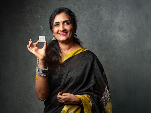
Jaya Jagadish, Country Head, AMD India & SVP Silicon Design Engineering, AMD
Image: Nishant Ratnakar for Forbes India
Advertisement
In 2016, about 12 years into the establishment of chip maker AMD’s design team in India, Jaya Jagadish and a team of about 150 engineers were entrusted with a CPU IP for a Sony game console. The project from such a prestigious client had come at a time when Jaya’s team were working on another project that was dragging on. With the customer’s own schedule at stake—and the possibility that they could pull out—an insane four months ensued that started with a lot of scepticism.
“There was a lot to prove, even for us. I mean, a remote team in India, a woman as a leader... there was scepticism all around," Jaya recalls.
But Jaya, who was senior director of design engineering at the time, insisted on complete transparency, both internally and with the customer, every step of the way: It was a new process, and they’d do everything in their power to deliver, but semiconductor design is tricky and a humongous challenge at the best of times.
When that design was wrapped up successfully, the mood turned into one of admiration and respect, and the desire to do more work with this team, she recalls. Many on that team have gone on to do bigger, greater things. And that’s the kind of experience that has now led to the growth of the team and also the change in approach towards what could be done from India, she says. “We proved that India can take on ownership and deliver in spite of the difficult challenges."
And as it became apparent that such experiences were not one-offs but the norm, it paved the way for more ownership and more growth, through this. Jaya is today country manager and senior vice president at AMD India, leading the chip maker’s biggest global design team anywhere, including the US.
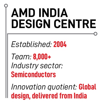
Today, AMD’s India design team, which started with a handful of engineers on Bengaluru’s Richmond Road 20 years ago, has more than 7,000 engineers in 10 different design centres in India, in total occupying about 1.5 million sq ft of office space. By 2028, AMD expects to hit 10,000 plus.
And the ownership is coming. Jaya and the team in India have just started working on a “roadmap core" CPU, meaning one of the mainstream CPUs that AMD is looking to bring to market within roughly the next three years. “The entire team will be working on it. I can’t divulge too much about the design aspects, but it is one of the roadmap cores and that’s hugely exciting" she says. “After 20 years, that feels like a great milestone to reach."
In the world of semiconductors, indeed it is. “So, it’s not just about the headcount but a testimonial to how India’s expertise or value-add to AMD’s overall growth has grown."
Building the CPU team was her first assignment when she moved to AMD India from the US almost 20 years ago. Back then, the talent was not readily available, and she had to focus on hiring sharp engineers and training them. Today that team is a 500-plus strong team. And AMD India boasts ‘senior fellow’- and ‘technical fellow’-level scientists and engineers in multiple areas.
Typically, main cores are produced one every three years. But they also need variants incorporating different features—a security feature, or different-sized memory or caches, for example. These are efforts that the India teams take over. Today they’re poised to take on full ownership of a next-generation CPU core itself.
Similarly, with systems-on-chips or SoCs, AMD’s India design team includes a full-fledged SoC team “spinning various resources and taping out from India", Jaya says. Confidence in India’s capabilities was validated when in 2023, AMD announced a $400 million investment in India.
AMD’s India engineers have also contributed to its AI accelerator chips, Jaya says, spanning hardware, software both in terms of IP development and SoC development. In semiconductor parlance, ‘IP’ refers to reusable design components or building blocks that can be integrated into semiconductor chips. Memory controllers or interfaces (USB, for instance) are examples of such IP.
The next 10 years will be a defining period for the whole semiconductor industry, she says. There was a time, when she started her own career, “I used to have a hard time explaining to my friends and family what I really do. You know, other than being clubbed with IT or testing, it was hard for them to understand," she says.
Today chip design has surfaced as a major industry and the growth can only be great for India because of the base that has been built, the strength of the engineering teams and ease of doing business in India with the various government initiatives and incentive plans. The growing startup ecosystem, the emphasis on manufacturing, all of this will come together over the next 10 years, she says.
 When that design was wrapped up successfully, the mood turned into one of admiration and respect, and the desire to do more work with this team, she recalls. Many on that team have gone on to do bigger, greater things. And that’s the kind of experience that has now led to the growth of the team and also the change in approach towards what could be done from India, she says. “We proved that India can take on ownership and deliver in spite of the difficult challenges."